Make PCB with Photoresist Film
Project Overview: PCB Fabrication Using Photoresist Film
In this project, we demonstrate the process of creating a printed circuit board (PCB) using photoresist film. This method ensures high precision and is ideal for prototyping or small-scale PCB production. The process involves several key stages, including surface preparation, photoresist application, UV exposure, etching, and finishing. Below is a detailed and professional explanation of each step:
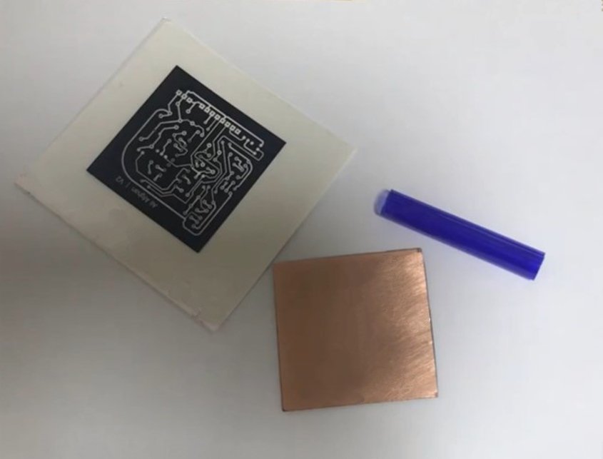
Step 1: PCB Design and Printing
-
PCB Design:
- Use PCB design software (e.g., Eagle, Altium, or KiCAD) to create the circuit layout.
- Ensure the design meets required specifications, including trace widths and spacing.
-
Print the Design:
- Export the design and print it onto transparent film using a laser printer. The black areas represent conductive traces, and the clear areas indicate where copper will be removed.
- For better results, use a high-resolution printer to ensure sharp and precise lines.
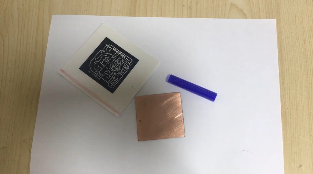
Step 2: PCB Preparation
-
Surface Preparation:
- Start with a clean copper-clad PCB. Sand the surface lightly with fine-grit sandpaper to remove oxidation and ensure smoothness.
- Wash the PCB thoroughly with water and soap, and dry it completely.
-
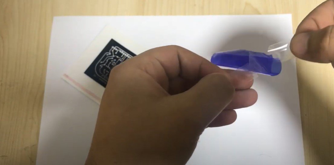
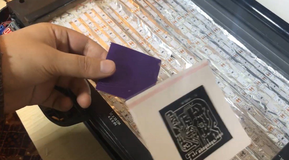
Apply Photoresist Film:
- Separate the protective backing from the photoresist film using adhesive tape.
- Carefully apply the film onto the PCB, ensuring there are no air bubbles or wrinkles.

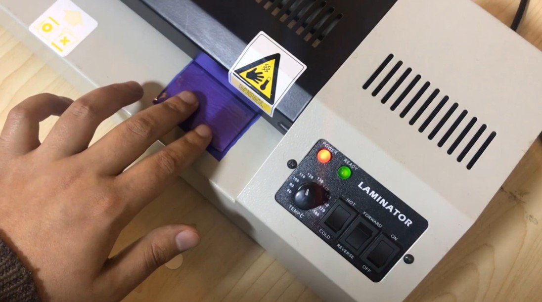
-
Laminate the Film:
- Use a laminator or apply even pressure and heat to secure the film firmly to the PCB surface. This ensures a smooth and uniform bond between the film and the copper layer.
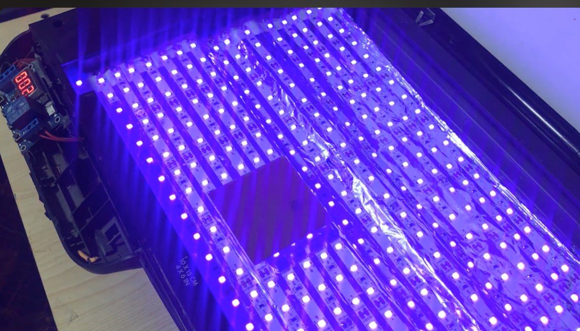
Step 3: UV Exposure
-
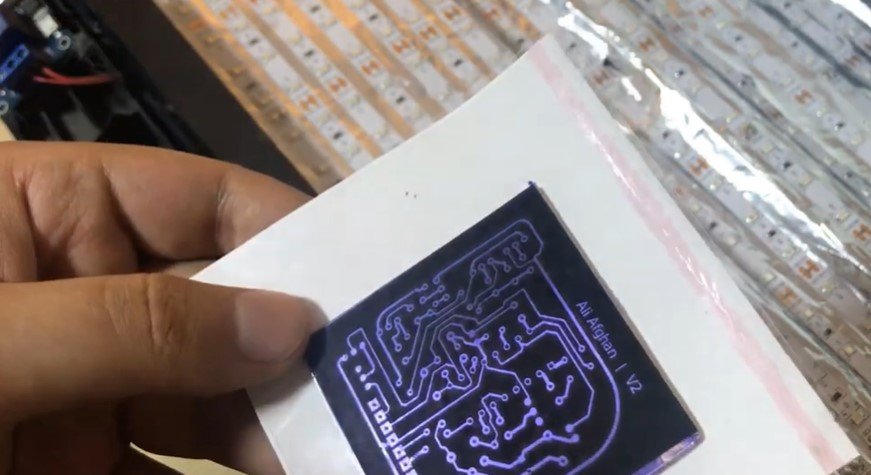
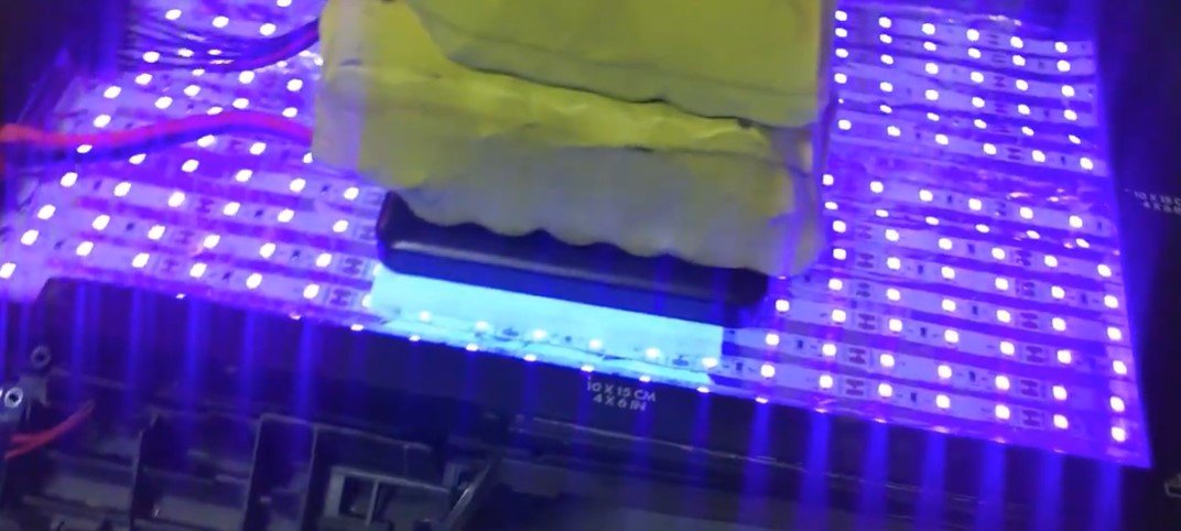
Align the Printed Film:
- Place the printed transparent film over the photoresist-coated PCB, ensuring precise alignment.
-
UV Exposure:
- Expose the PCB to UV light for a specific duration (as recommended by the photoresist film manufacturer).
- The UV light hardens the areas exposed through the clear parts of the film, while the black areas remain unaffected.


Step 4: Developing the PCB
-
Remove Protective Layer:
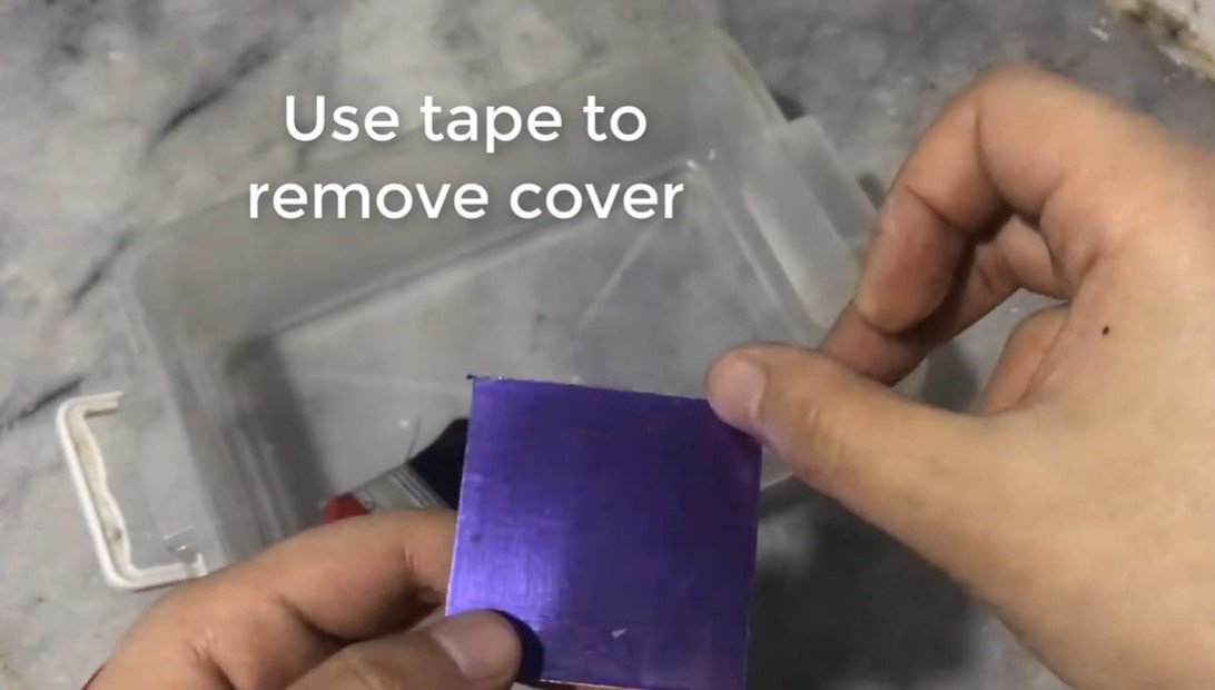
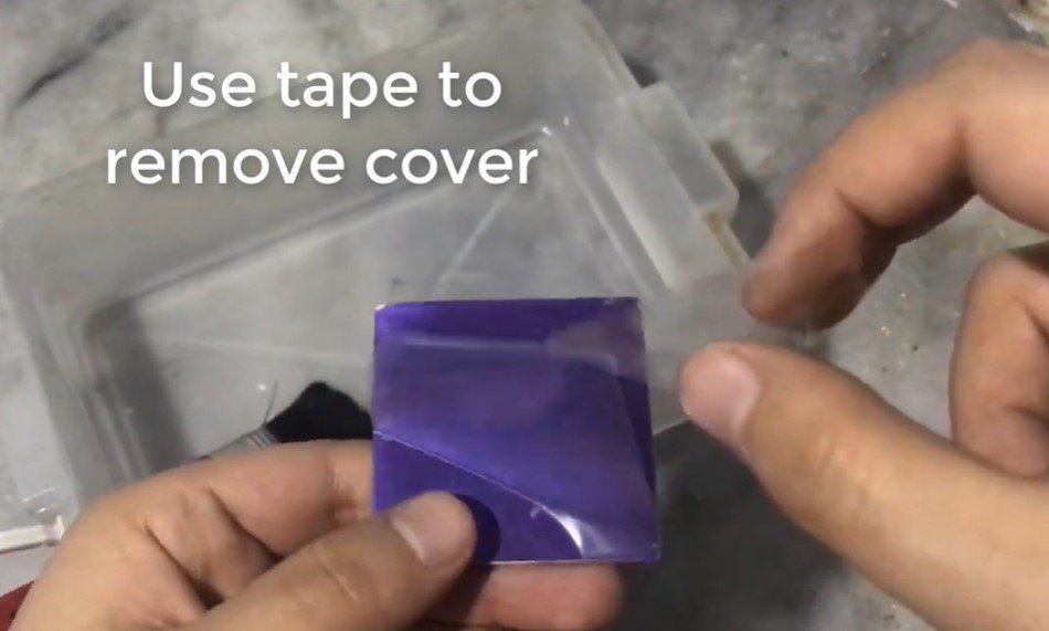
- After UV exposure, peel off the top protective layer of the photoresist film using adhesive tape.
-
Develop the Image:
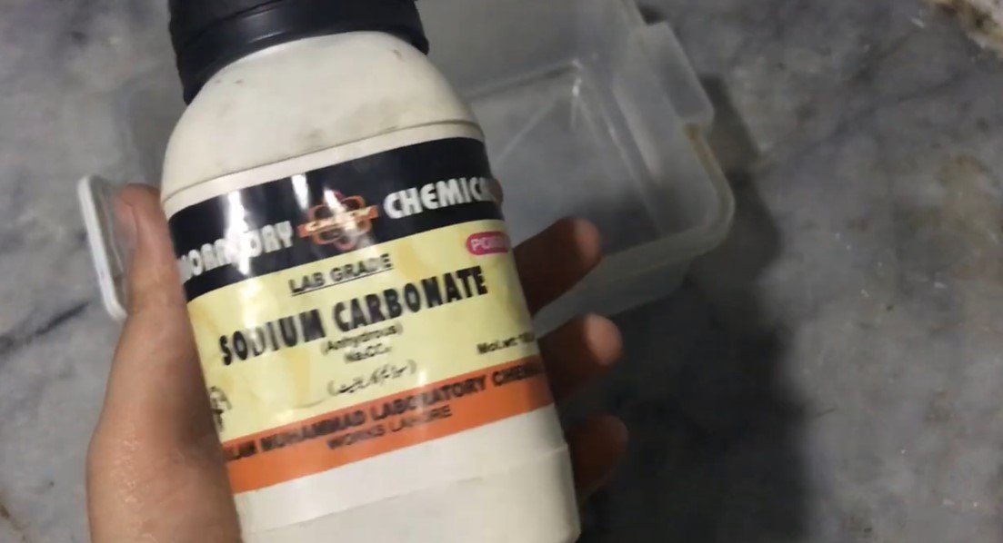
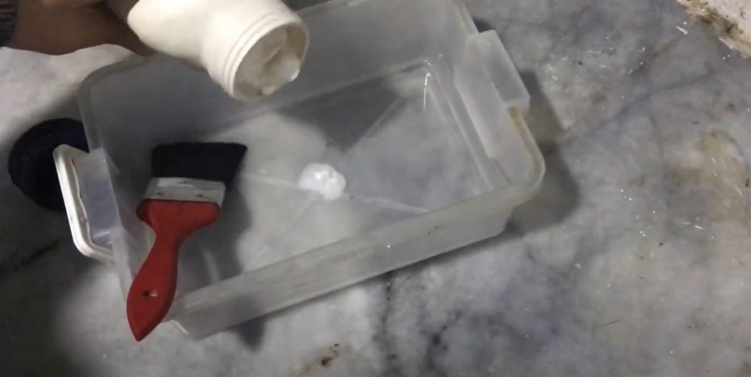
- Prepare a solution of sodium carbonate (Na₂CO₃) in water.
- Submerge the PCB in the solution and gently brush to remove the unexposed (unhardened) areas of the film, revealing the bare copper underneath.
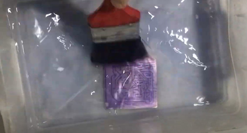
-
Final UV Hardening:
- Once the desired areas are exposed, place the PCB back under UV light for additional hardening of the remaining photoresist.


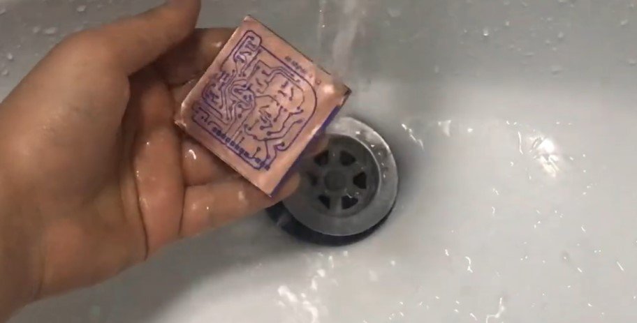
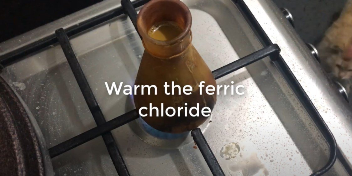
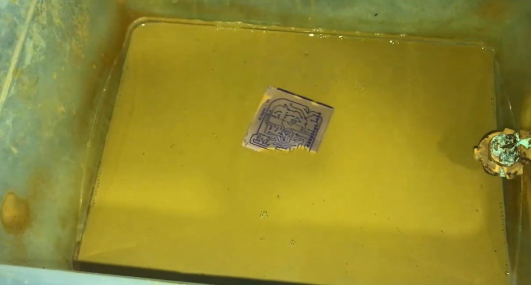
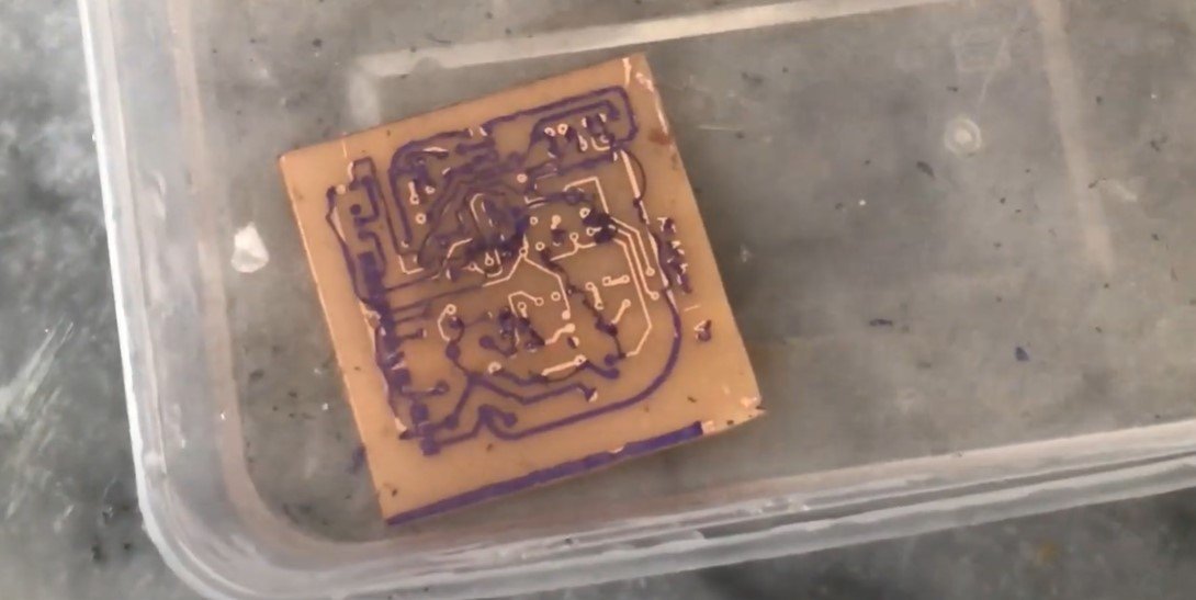
Step 5: Etching the PCB
-
Prepare Ferric Chloride Solution:
- Heat ferric chloride (FeCl₃) solution to improve the etching process.
- Use appropriate safety measures, such as gloves and goggles, as ferric chloride is corrosive.
-
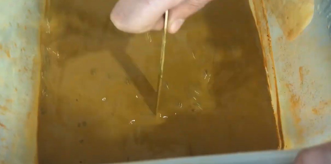
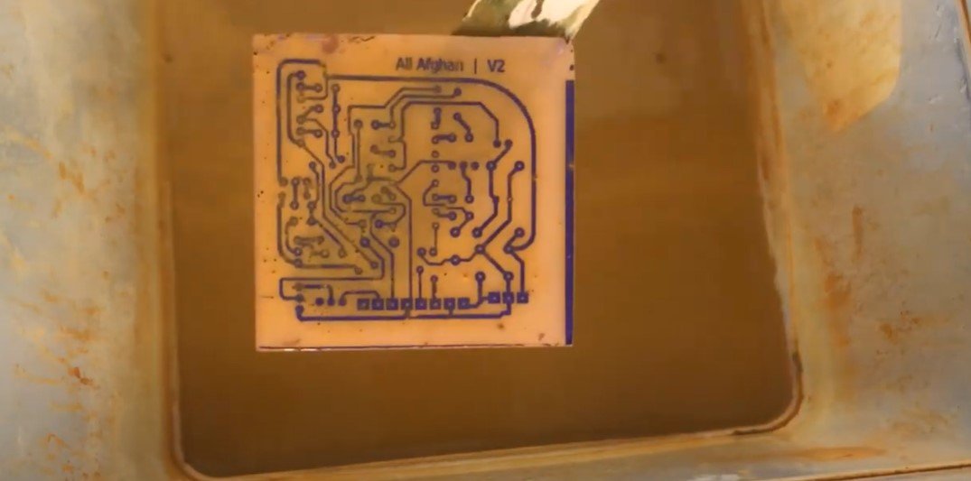
Etch the PCB:
- Submerge the PCB in the ferric chloride solution and agitate gently to speed up the etching process.
- Continue until all the exposed copper is dissolved, leaving only the traces protected by the hardened photoresist.
-
Rinse the PCB:
- Wash the PCB thoroughly with water to remove any remaining etchant.
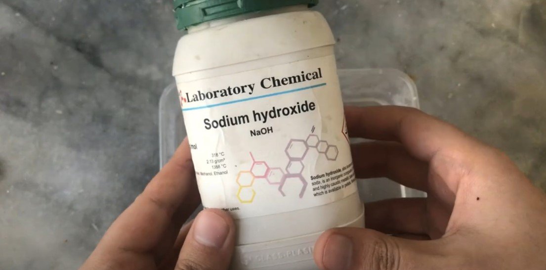
Step 6: Removing the Photoresist
-
Prepare Sodium Hydroxide Solution:
- Mix sodium hydroxide (NaOH) with water to create a stripping solution.
-
Remove the Photoresist:
- Submerge the PCB in the solution to dissolve the hardened photoresist.
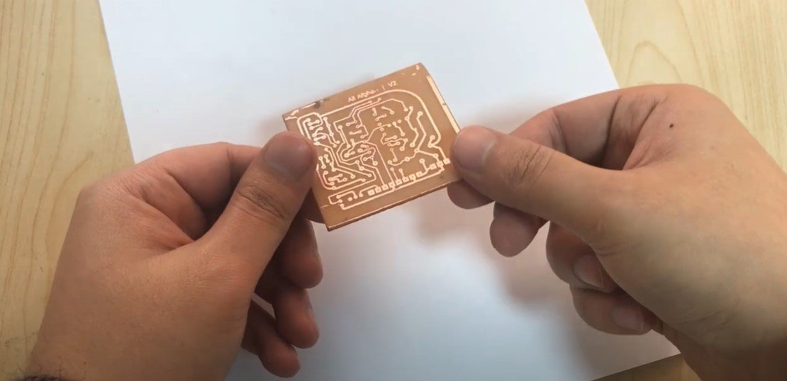
- Wash the PCB with water to reveal the final copper traces.
Step 7: Drilling and Component Soldering
-
Drill Holes:
- Use a precision drill to create holes for through-hole components as per the PCB layout.
-
Component Assembly:
- Solder the components onto the PCB using a soldering iron and appropriate solder wire.
- Check connections for continuity and functionality.
Benefits of Photoresist PCB Fabrication
-
High Precision:
- Photoresist film allows for detailed and accurate trace patterns.
-
Cost-Effective:
- Ideal for prototyping and small-scale production without the need for professional equipment.
-
Customizable:
- Enables easy adjustments to the PCB design for unique project requirements.
Conclusion
Using photoresist film to fabricate PCBs is an efficient and reliable method for creating high-quality boards. By following the outlined steps carefully, you can produce PCBs suitable for a wide range of electronic applications. This process is perfect for DIY enthusiasts, electronics hobbyists, and engineers working on prototypes or small-batch production.
Posted by Ali Aslan at Friday 10th of January 2025 11:40:47 AM