DIY DC To DC Boost Converter
DIY DC To DC Boost Converter
A boost converter (step-up converter) is a DC-to-DC power converter that steps up voltage (while stepping down current) from its input (supply) to its output (load). It is a class of switched-mode power supply (SMPS) containing at least two semiconductors (a diode and a transistor) and at least one energy storage element: a capacitor, inductor, or the two in combination. To reduce voltage ripple, filters made of capacitors (sometimes in combination with inductors) are normally added to such a converter's output (load-side filter) and input (supply-side filter).
History
For high efficiency, the switched-mode power supply (SMPS) switch must turn on and off quickly and have low losses. The advent of a commercial semiconductor switch in the 1950s represented a major milestone that made SMPSs such as the boost converter possible. The major DC to DC converters were developed in the early 1960s when semiconductor switches had become available. The aerospace industry’s need for small, lightweight, and efficient power converters led to the converter’s rapid development.
Switched systems such as SMPS are a challenge to design since their models depend on whether a switch is opened or closed. R. D. Middlebrook from Caltech in 1977 published the models for DC to DC converters used today. Middlebrook averaged the circuit configurations for each switch state in a technique called state-space averaging. This simplification reduced two systems into one. The new model led to insightful design equations which helped the growth of SMPS.
Operation
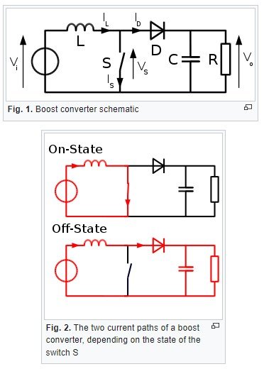
The key principle that drives the boost converter is the tendency of an inductor to resist changes in current by either increasing or decreasing the energy stored in the inductor magnetic field. In a boost converter, the output voltage is always higher than the input voltage. A schematic of a boost power stage is shown in Figure 1.
- When the switch is closed (on-state), current flows through the inductor in the clockwise direction and the inductor stores some energy by generating a magnetic field. Polarity of the left side of the inductor is positive.
- When the switch is opened (off-state), current will be reduced as the impedance is higher. The magnetic field previously created will be reduced in energy to maintain the current towards the load. Thus the polarity will be reversed (meaning the left side of the inductor will become negative). As a result, two sources will be in series causing a higher voltage to charge the capacitor through the diode D.
If the switch is cycled fast enough, the inductor will not discharge fully in between charging stages, and the load will always see a voltage greater than that of the input source alone when the switch is opened. Also while the switch is opened, the capacitor in parallel with the load is charged to this combined voltage. When the switch is then closed and the right hand side is shorted out from the left hand side, the capacitor is therefore able to provide the voltage and energy to the load. During this time, the blocking diode prevents the capacitor from discharging through the switch. The switch must of course be opened again fast enough to prevent the capacitor from discharging too much.
The basic principle of a boost converter consists of 2 distinct states (see figure 2):
- In the on-state, the switch S (see figure 1) is closed, resulting in an increase in the inductor current;
- In the off-state, the switch is open and the only path offered to inductor current is through the flyback diode D, the capacitor C and the load R. This results in transferring the energy accumulated during the on-state into the capacitor.
- The input current is the same as the inductor current as can be seen in figure 2. So it is not discontinuous as in the buck converter and the requirements on the input filter are relaxed compared to a buck converter.
Continuous mode
When a boost converter operates in continuous mode, the current through the inductor (��) never falls to zero. Figure 3 shows the typical waveforms of inductor current and voltage in a converter operating in this mode.
 ) never falls to zero. Figure 3 shows the typical waveforms of inductor current and voltage in a converter operating in this mode.
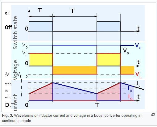
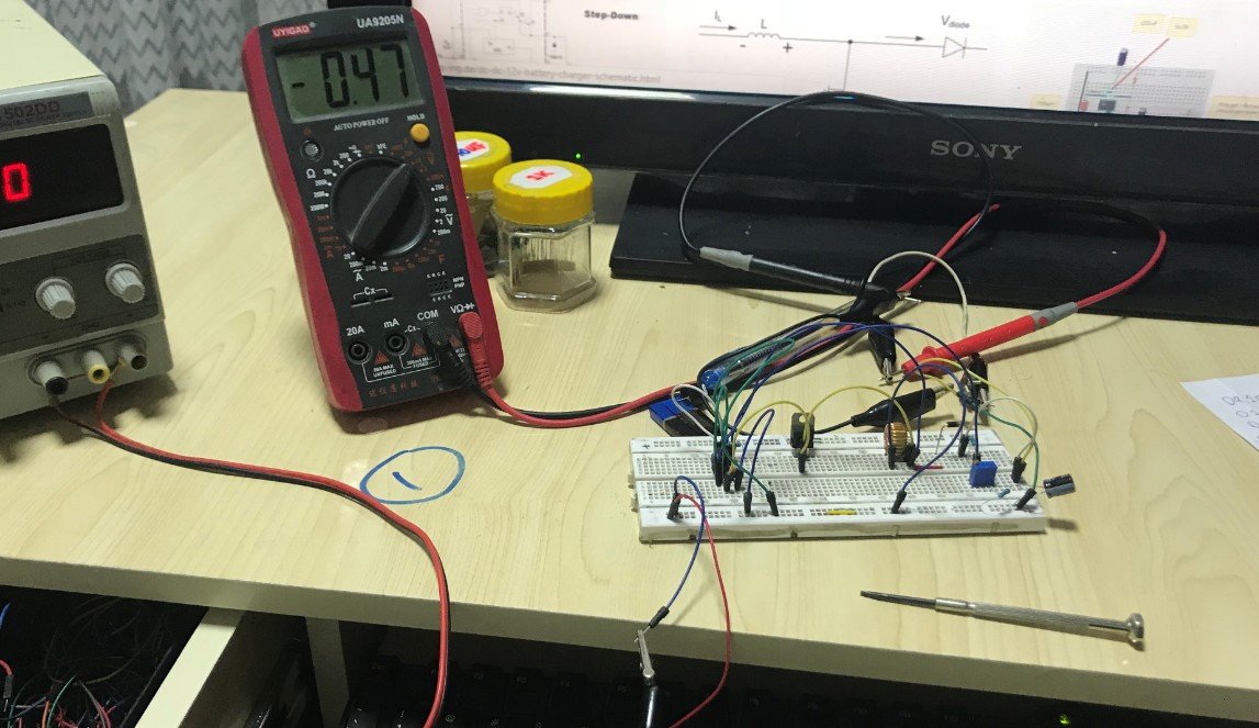
Build the Circuit!
Here you can find the schematic for the project.

Upload the Code!
In order to upload the code to the ATtiny85 you can use an Arduino Uno.
Success!
You did it! You just created your own Boost Converter!


Posted by Ali Aslan at Tuesday 9th of May 2023 08:40:54 PM